Redrawing the echo hello-world board
Original circuit
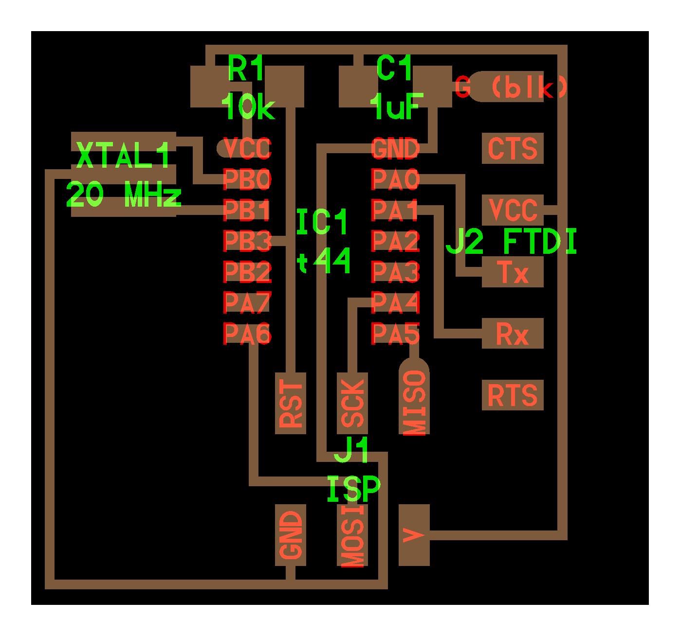
- IC (Attiny44) connected to a crystal that consists of built-in capacitors.
- A current limiting reistor that is connected to the vcc of the IC
- A decoupling capacitor connected from Vcc to ground
Working with Eagle
Since this is the first time I am working on Eagle, it was a bit challenging to get used to as any other program. But once I got a hang of it, it felt a bit easier to use than the other PCB design softwares I used previously.In order to get the components needed to design the circuit, I downloaded the fab library from here.
The next steps were just adding the components and connecting them (connections can be done either by using wires or labels).
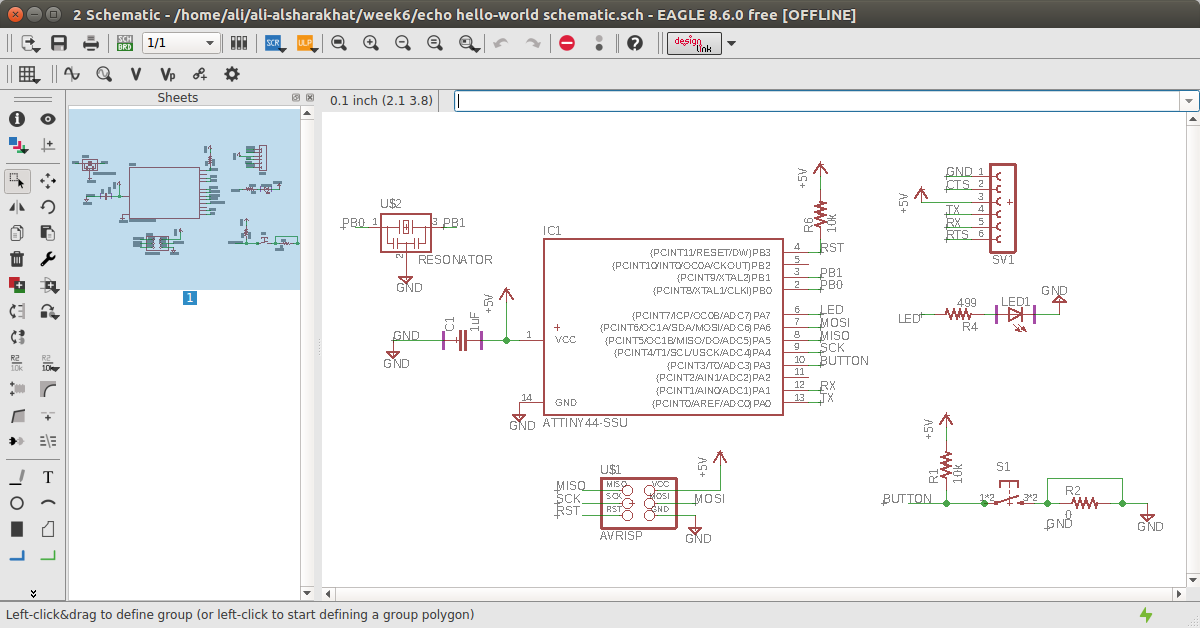
Circuit schematic
To my final board, I have added a LED to PA7 instead of directly connecting to Vcc, which would allow me to control the LED blink through the micro-controller. The next section exlains how the resistance value was obtained.For the switch, I have connected it with a pull-up resistor, which makes the microcontroller read the input as high when the button is not pressed, and when the button is pressed, the current will flow through the resistor to ground hence giving a low input to the pin.
Adding an LED
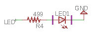
Calculating the current limiting resistor
R = (Vs-Vled)/IledWhere:
- R -> Current limiting resistor's resistance
- Vs -> Supply voltage
- Vled -> Forward Voltage of the LED
- Iled -> Forward Current of the LED
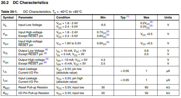
The supply voltage comes as an output from the ATtiny44's pins. The voltage value can be determined from the IC's datasheet here, which is 4.3V as shown below.
Through the LED's datasheet here the following constants need to be determined:
- Forward current
- Forward voltage

R = (4.3-2)/0.02
R = 115 ohms
So, the current limiting resistor value that needs to be used is 115 ohms or greater.
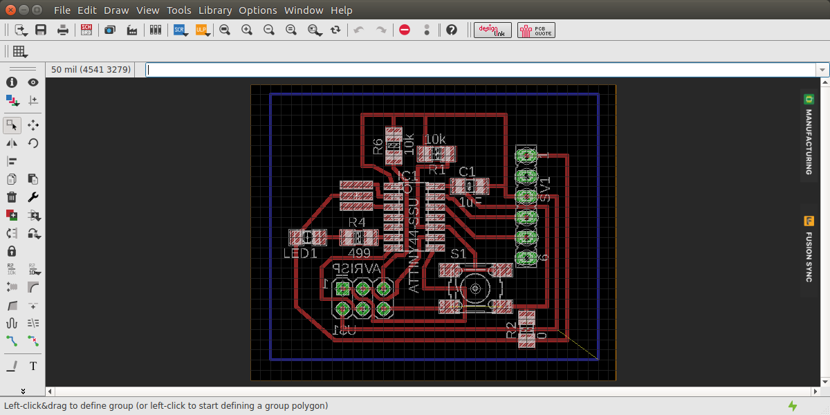
PCB design
After completing the schematic design, the next thing is arranging the components for PCB printing. This is something that is frustrating for some people and fun for others, since it can be compared to a puzzle that you want to complete with the leaest number of jumpers.While designing my PCB, I made use of the switch that consisted of 4 pins but it had only 2 actual ones since 2 pins are internally shorted, which made the switch act as a large jumper.
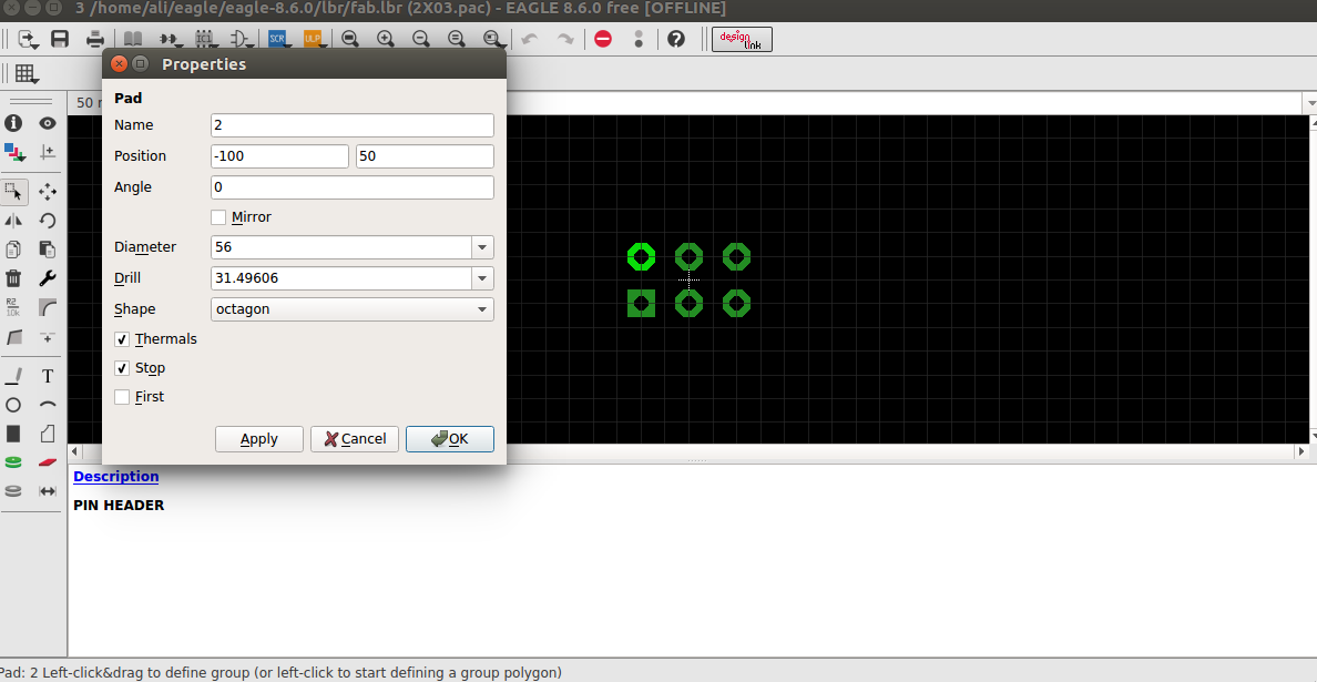
One issue we had was that at that time we only had a few surface mount male and female headers, so some of us had to use through hole headers. Another issue was that the diameter of the pins in the library were different from the actual, so we had to measure the actual diameter and change the one stated in the library (Right click on the part->open package).
After finishing the design, to make things easier for the cutout, I have added a wire on the bottom layer that outlines the PCB.
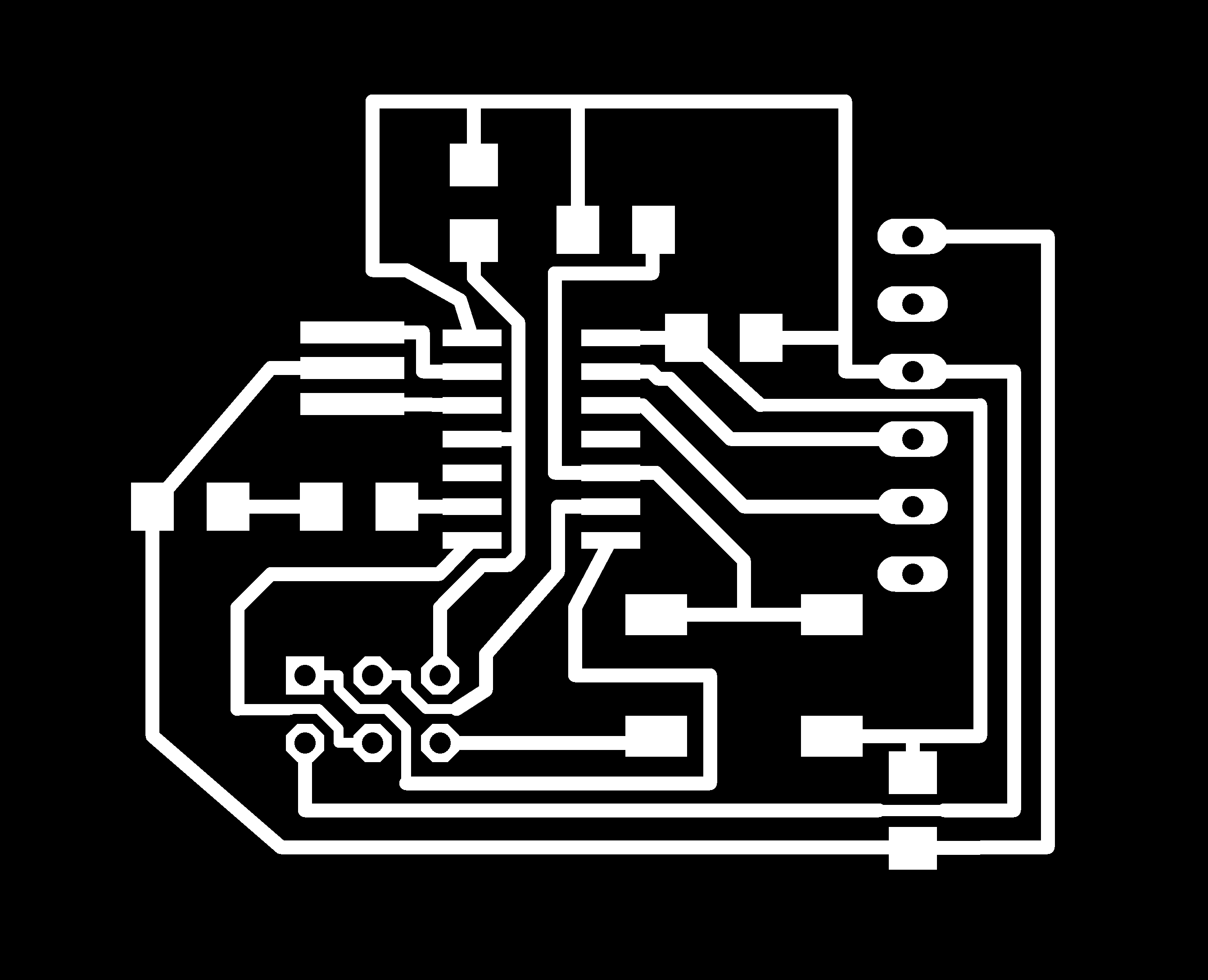
The image below shows the png file for the traces. The selected layers were top and pads.
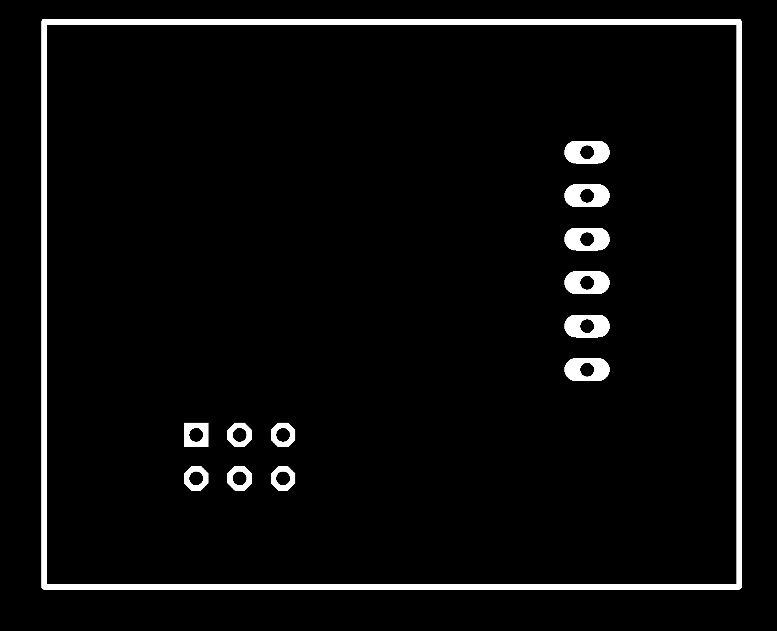
For the cutout png file, the selected layers were pads and bottom. The file is then edited in inkscape (the black area in the middle is changed to white) (note: white represents the traces).
Circuit after soldering
Programming and testing